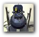
SOLVER P47
Atomic Force Microscope (AFM) and Scanning Tunneling Microscope (STM), NT-MDT
It allows the study of the properties and surface topography of nanomaterials on the micro and nano scale, with particular emphasis on the measurement of friction forces and the characteristics of self-organizing materials.
AFM:
General capabilities:
Determination of the surface topography of metallic, ceramic, polymer and composite materials. Characterization of nanoobjects and nanometer structures. Testing of friction, wear, adhesion and capillary forces at the nano and micro levels.
Specific applications:
1. Thin organic layers and polymers
- Research on thin and ultrathin layers and monolayers of organic compounds on various metallic and ceramic substrates - measurement of layer thickness, friction testing at the nano- and micro-scale.
- Characterization of topography and testing of frictional and mechanical properties of polymers (e.g. polyurethanes, polymethacrylates, silicone polymers) and other commonly used materials and polymer composites. (e.g. for biological applications: catheters, dressing materials, etc.)
2. Thin ceramic and metallic layers
- Topography studies and friction characteristics of ceramic layers obtained by sol-gel, dip-coat methods, sputtered layers, plasma-deposited layers, CVD/PVD layers
3. Research on magnetic materials
- Determination of domain structure in magnetic materials
4. Tests and research of information media
- Analysis of CD/DVD disks and other data carriers with magnetic information recording
5. Research on the mechanical properties of nanoobjects
- Measurements of the Young's modulus of carbon nanotubes
6. Biological research
- Visualization of biological macromolecular systems, examination of collagen structures, erythrocytes, DNA strands, etc.
STM:
General capabilities:
Determination of the surface topography of conductive materials. Characterization of nanoobjects and nanostructures with atomic resolution
Specific applications:
- Imaging of SAM-type reconstruction nanocomposite materials placed on a gold surface
- Morphological imaging of the electronic properties of carbon nanotubes
- Nanoparticle analysis
- Determination of structures in thin layers of organic semiconductors from the thiol group
- Observation of adsorption layers of organic compounds from solutions on the surfaces of electrically conducting materials
- Characterization of topography of ceramic layers obtained by the CVD/PVD method
- Characterization of nanostructures of conductors and semiconductors using STM/STS