- University of Lodz
- Faculty of Chemistry
- Department of Materials Technology and Chemistry
- Experimental techniques and apparatus
- Scanning Electron Microscopy (SEM)
Scanning Electron Microscopy (SEM)
Nova NanoSEM 450, FEI
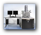
Scanning electron microscope with EDS analyzer
High-resolution scanning electron microscope SEM, equipped with an electron gun with thermal field emission (Schottky emitter) with an accelerating voltage adjustable in the range from a minimum of 200 V to 30 kV. The microscope works in high vacuum mode of 6*10-6 mbar and in low vacuum mode (<2 mbar). Depending on the measurement parameters used, it is possible to achieve high resolutions (up to 1 nm).
The microscope is equipped with a number of detectors allowing the observation of the surface topography using secondary electrons (SE) and backscattered electrons (BSE) signals. These detectors include:
-
TLD intra-lens detector, with the ability to operate in two immersion modes, recording the secondary electron signal (SE) and the backscattered electron signal (BSE)
-
ETD detector mounted in the SEM chamber to work in the basic mode, recording the secondary electrons (SE) signal
-
LVD detector for operation in low vacuum conditions, directly recording the secondary electron (SE) signal
-
Highly sensitive CBS detector with 4 sectors arranged concentrically, enabling the detection of backscattered electrons (BSE), compatible with the electron energy slowing down mode
-
Highly sensitive STEM transmitted electron detector with the ability to observe in bright field (BF), dark field (DF) and wide-angle dark field (HAADF).
In addition, the FEI Nova NanoSEM 450 microscope is equipped with an X-ray EDS spectrometer with a large active surface (60 mm2), enabling the detection of elements from boron upwards. The SEM/EDS system provides the possibility of qualitative analysis of samples in terms of elemental composition: point-wise, from a selected reduced area, from the entire frame, along any line (linescan) and the distribution of elements in a selected area (X-ray mapping). The EDS system has the ability to collect X-ray maps of at least 30 elements at the same time.
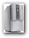
Phenom G2 Pure
 The Phenom G2 Pure electron microscope is a tool for the initial characterization of specimens intended for research using a scanning electron microscope (SEM), which requires a smooth transition from imaging in the optical microscope mode to imaging in the electron microscope mode while ensuring high image quality.
Basic features of the system:
- Resolution: 7,8 nm
- Imaging modes:
- optical: constant magnification of 20x
- electron beam: magnification of 70÷17,000x
- Recording of digital images:
- optical mode: color camera
- eletron beam mode: highly sensitive backscattered electron detector
- Image processing module, 17-inch touch monitor, control knob, diaphragm vacuum pumps, power supply, USB 2.0 Flash
- Image saving formats: JPEG, TIFF, BMP